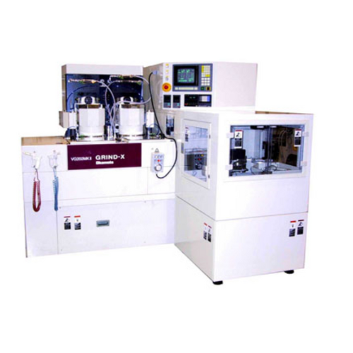
Ultra accurate back grinder SVG202MKⅡ
_____________________________________________________________________________________________________________________
SERIES line-up
SVG202MKⅡ _________________________________________________________________________________________________________________________________CONCEPT
SOI and Bonded wafer dedicated grinder. __________________________________________________________________________________________________________________________________Feature
- Specialized grinder designed for SOI wafers requiring ultimate Total Thickness Variation (TTV) control.
- Components are made from low-expansion materials to prevent thermal deformation and ensure consistent performance over time.
- Optional soft wafer removal control system enables submicron-level layer thickness precision, unaffected by substrate thickness variations.
Uses of Ultra-Accurate Back Grinder SVG202MKⅡ
- Wafer Thinning: Reduces wafer thickness for semiconductor packaging like flip-chip and 3D stacking.
- High Precision: Ensures ultra-accurate grinding with minimal damage.
- Material Compatibility: Processes silicon, SiC, GaAs, and other advanced materials.
- 3D Integration Support: Prepares wafers for TSVs and 3D chip designs.
- MEMS & Sensor Fabrication: Enables ultra-thin wafers for MEMS and sensor devices.
- Yield Optimization: Minimizes breakage and ensures consistent quality across batches.
- Customizable Processes: Offers variable wafer thickness and integrates with other production steps.