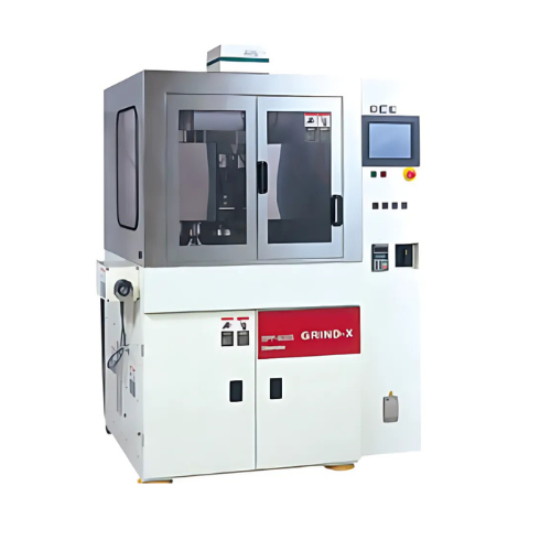
CMP-Chemical mechanical polishing-SPP600S
_____________________________________________________________________________________________________________________
SERIES line-up
SPP600S・SPP800S・SPP1000S・SPP1200S _________________________________________________________________________________________________________________________________CONCEPT
User friendly design for environment and usability. __________________________________________________________________________________________________________________________________Feature
- Manual CMP for R&D:
- Designed for research and development purposes with manual operation.
- User-Friendly Display:
- Features an intuitive display to check the current process status in real time.
- Stable Data Collection:
- Includes a primary time-setting function for reliable data collection.
- Collected data can be used with the fully automatic polisher PNX332B.
- Uniformity Preservation:
- Maintains wafer uniformity even after more than 10µm material removal.
- Dedicated Dresser Unit:
- Comes with a dedicated dresser unit, with an option to replace with a diamond dresser.
- Environmentally Friendly Design:
- Incorporates a slurry recycling system to reduce waste and environmental impact.
Uses of CMP (Chemical Mechanical Polishing) SPP600S
- Semiconductor Wafer Polishing:
- Used for polishing silicon wafers in semiconductor manufacturing to achieve smooth and uniform surfaces for photolithography and device fabrication.
- Flatness Enhancement:
- Improves the flatness and planarity of wafers by removing surface defects and irregularities, essential for advanced microelectronics.
- Chemical and Mechanical Surface Treatment:
- Combines chemical etching with mechanical abrasion for precise control over wafer surface finishing.
- Polishing of Compound Materials:
- Suitable for polishing compound semiconductor materials such as sapphire, SiC, and GaAs for optoelectronic and high-power devices.
- MEMS Fabrication:
- Used in the production of microelectromechanical systems (MEMS) to achieve smooth, uniform surfaces for sensors and actuators.
- Optical Surface Finishing:
- Polishes optical substrates (such as lenses and mirrors) to achieve high-quality, defect-free surfaces.
- Integration with R&D and Production:
- Ideal for both research and development settings, as well as mass production, ensuring high precision in both environments.
- Multi-Wafer Batch Processing:
- Enables the processing of multiple wafers simultaneously, increasing productivity in high-volume manufacturing.