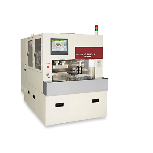
200mm back grinder GNX200B
_____________________________________________________________________________________________________________________
SERIES line-up
GNX200B・GNX300B _________________________________________________________________________________________________________________________________CONCEPT
Back grinder best seller __________________________________________________________________________________________________________________________________Feature
Features an index table and down-feed grinding, making it a best-selling back grinder. Supports various processes by incorporating a coin stack unit and stress relief equipment, ensuring flexibility to adapt to evolving process requirements.Uses of the 200mm Back Grinder GNX200B
- Wafer Thinning for Semiconductor Devices
- Precisely grinds 200mm wafers to ultra-thin dimensions, supporting the production of advanced semiconductor devices.
- MEMS Fabrication
- Ideal for thinning wafers used in Micro-Electro-Mechanical Systems (MEMS) to meet strict dimensional and cleanliness requirements.
- TSV Applications
- Supports silicon via (TSV) processes by enabling ultra-thin wafer grinding with high surface quality.
- LED and Optoelectronic Components
- Suitable for manufacturing wafers used in LEDs, sensors, and other optoelectronic applications requiring thin and high-quality substrates.
- High-Density Packaging
- Enables wafer thinning for 3D integrated circuit packaging, supporting high-speed and compact electronic device designs.
- Stress Relief Processing
- Equipped to handle stress relief processes to ensure wafer reliability and prevent warping during subsequent stages.
- R&D and Prototyping
- Widely used in research and development facilities for testing and prototyping advanced semiconductor manufacturing techniques.