300mm Ultra thin wafer polisher GNX12PB
_____________________________________________________________________________________________________________________
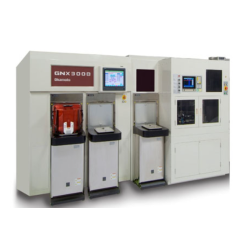
SERIES line-up
GNX8PB/GNX12PB _________________________________________________________________________________________________________________________________Feature
- Utilizes an air back pressure system and scanning polish to evenly remove grinding damage.
- Optional coin stack unit available, ideal for processing thin wafers.
- Can operate as a stand-alone machine or as part of an in-line system with the grinder, accommodating various low-volume product requirements.
Uses of the 300mm Ultra-Thin Wafer Polisher GNX12PB
- Surface Refinement for Semiconductor Wafers
- Delivers ultra-smooth, high-quality surfaces, essential for advanced semiconductor device manufacturing.
- Post-Grinding Damage Removal
- Effectively removes grinding-induced damage, ensuring superior wafer integrity and reliability.
- 3D IC and TSV Applications
- Supports Through-Silicon Via (TSV) and 3D integrated circuit packaging processes by providing exceptional surface flatness.
- Thin Wafer Processing
- Optimized for ultra-thin wafers, meeting the demands of high-performance, compact semiconductor devices.
- MEMS and Optoelectronics
- Ideal for Micro-Electro-Mechanical Systems (MEMS) and optoelectronic components, where precision and surface quality are critical.
- Stress Relief and Warpage Minimization
- Polishes wafers to relieve stress and minimize warpage, enhancing downstream process stability.
- Customization for Various Applications
- Suitable for diverse applications in semiconductor R&D, low-volume production, and high-end manufacturing environments.