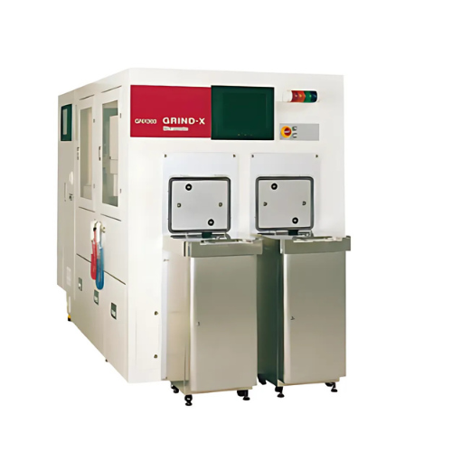
300mm back grinder GNX300B
_____________________________________________________________________________________________________________________
SERIES line-up
GNX200B・GNX300B _________________________________________________________________________________________________________________________________CONCEPT
Back grinder best seller __________________________________________________________________________________________________________________________________Feature
- Recognized as a best-selling back grinder due to its superior performance and reliability.
- Features an index table for efficient wafer handling and precise positioning.
- Incorporates down-feed grinding technology for high-accuracy wafer thinning and surface quality.
Uses of the 300mm Back Grinder GNX300B
- Wafer Thinning for Advanced Semiconductor Devices
- Enables precise grinding of 300mm wafers, supporting the production of cutting-edge semiconductor technologies.
- 3D Packaging and TSV Applications
- Facilitates Through-Silicon Via (TSV) and 3D integrated circuit (IC) packaging processes by achieving ultra-thin wafer dimensions with exceptional surface quality.
- MEMS Manufacturing
- Ideal for producing thin wafers required for Micro-Electro-Mechanical Systems (MEMS) with strict cleanliness and thickness specifications.
- Optoelectronic Device Production
- Supports the fabrication of wafers used in LEDs, sensors, and other optoelectronic applications requiring thin, high-quality substrates.
- Stress Relief and Warpage Control
- Equipped to perform stress relief processes, minimizing wafer warping and enhancing reliability for downstream applications.
- High-Volume Production
- Designed for high throughput and consistent performance, making it suitable for mass production in semiconductor manufacturing.
- Research and Development
- Widely used in R&D for prototyping and testing new semiconductor processes and devices.